




Moore’s Law gave semiconductor boards a predictable schedule to judge leaders against. That schedule has broken down. This article looks at how the CEO, CTO, COO, CFO, and CHRO roles are changing across eight business models, from integrated device manufacturers and foundries to chip IP licensors and equipment makers. The rebuild is hardest at IDMs and foundries, followed closely by OSATs. The CFO and CHRO roles have moved furthest from their old job descriptions. They need as much board attention as the CEO. Internal benches are thin. Boards will need to recruit across business models and from sectors such as defense, energy, pharmaceuticals, and large infrastructure. Before the next transition, boards should rewrite role specifications by business model, build benches two and three levels down, test succession plans against a compressed timeline, and check their own expertise against the profile they are hiring for.
For sixty years, Moore’s Law handed semiconductor boards a technical cadence so predictable that it could stand in for leadership judgment, and the cadence is thinning.
What Moore’s Law concealed, more than anything else, was the thinness of the industry’s senior leadership bench. A chip company could promote from within, reward technical depth, and trust that the steady two-year doubling of transistor counts would supply the remaining commercial context. Capital decisions were legible because the next node was legible, and hiring decisions were simple because technical credibility was the main thing boards needed to see. That entire set of assumptions is unraveling faster than most succession plans recognize, and the consequences are already visible inside active chief executive and chief operating officer searches, where the shortlist rarely contains the profile the conditions now require.
How the Drive for Moore’s Law Has Evolved in the Semiconductor Industry
The version of Moore’s Law that most board members still carry around in their heads, a doubling of transistor count every two years at predictable cost, has been fraying in public for close to a decade. Pat Gelsinger, former chief executive of Intel, conceded at the end of 2023 that effective doubling has slipped to roughly three years and that the golden era of straightforward transistor scaling is behind the industry. Research institutes like imec have set out the physical and economic limits pushing silicon toward a plateau. The IEEE’s framework for the future of devices and systems has since moved toward a “More than Moore” approach that treats system-level integration, rather than transistor count, as the organizing principle.
The physics underneath that plateau is worth naming, because the response to it is what matters most for leadership. As planar transistors shrank, the older MOSFET began to lose electrostatic control of its channel, with drain-induced barrier lowering and subthreshold leakage rising sharply. The industry answered with the FinFET, a three-sided fin that gave the gate better grip on the channel, which Intel introduced commercially at the 22-nanometer node in 2011. The FinFET stayed ahead of the problem through most of the 2010s. By the 2nm node even FinFETs were running out of margin. Electrons were tunneling across barriers they should have been unable to cross, and the copper interconnect wires carrying signals between transistors had fallen below the roughly forty-nanometer mean free path of electrons in copper, at which point their resistivity rose sharply as electron scattering took over. The industry answered a second time, with the gate-all-around transistor, in which the gate wraps the channel on all four sides instead of three, giving engineers near-ideal electrostatic control of the switch. TSMC’s N2 process, which entered volume production in late 2025, is the company’s first commercial node to use it, following Samsung’s pioneering introduction of the architecture at its 3nm node in 2022.
To explain this in a nontechnical way, a transistor is essentially a microscopic switch, and the gate is what opens and closes it. As engineers made transistors smaller and smaller over five decades, the on-and-off distance inside each switch eventually got so short that electrons stopped behaving predictably and began slipping through even when the switch was meant to be off, in the same way water will drip through a nearly-shut faucet no matter how hard you tighten it. At the same time, the tiny copper wires carrying signals between transistors got so thin that electrons moving through them started bumping into the walls of the wire itself, driving up resistance and wasting energy as heat. The FinFET was the industry’s first answer, giving the gate a three-sided grip on the channel to stop the leaks. The gate-all-around transistor is the second answer, wrapping the gate on all four sides. Each answer has required more engineering complexity than the last, and the numbers behind the current generation reveal why that matters commercially.
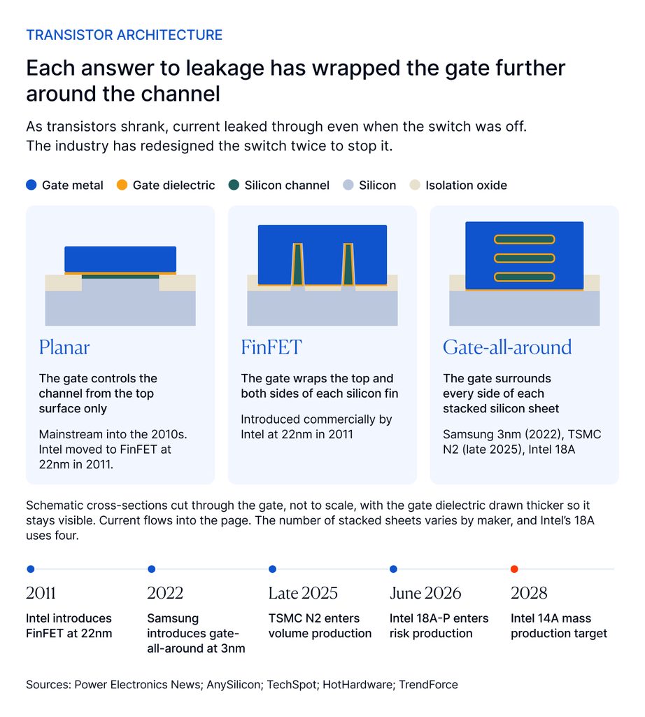
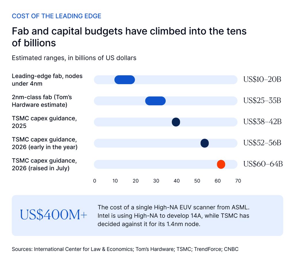
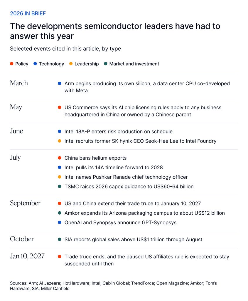
Where each new transistor generation used to bring a predictable gain from adding more transistors, backside power delivery plus gate-all-around now buys a performance improvement on the order of 10-15% at constant power, with the bulk of the benefit coming from reduced voltage droop and tighter standard-cell packing rather than from transistor count itself. Intel, which paired gate-all-around transistors with backside power delivery on its 18A node, announced in June 2026 that the enhanced 18A-P variant had entered risk production on the schedule promised to customers, delivering 9% more performance at the same power or an 18% reduction in power consumption at the same speed. In July, Intel pulled its 14A timeline forward by a year, with mass production now targeted for 2028. The cost of getting there, in capital and in time, has risen sharply. Leading-edge fabs for nodes under 4nm now cost between ten and twenty billion dollars each, and Tom’s Hardware estimates a 2nm-class fab at US$25 billion to US$35 billion. That climb is Rock’s Law, the companion observation to Moore’s that as chips grow denser the cost of making them rises exponentially, working in real time.
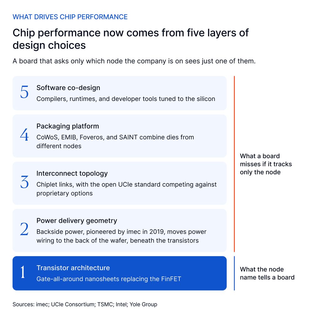
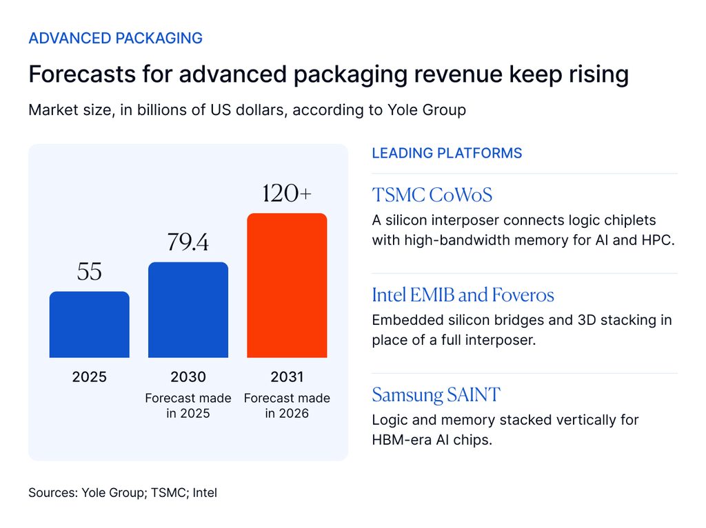
The industry’s answer to that cost pressure has been to stop relying on transistor scaling as the primary way to get more performance and to move the battle to the package. Advanced packaging, once a protective afterthought, has become the organizing principle for most high-performance product planning. Chiplet-based designs break the old monolithic system-on-chip into smaller dies optimized for different functions and reassemble them using 2.5D silicon interposers or 3D hybrid bonding. TSMC’s CoWoS platform uses a silicon interposer to connect logic chiplets with high-bandwidth memory for AI and high-performance computing (HPC) applications. Intel’s EMIB and Foveros do the same work using embedded silicon bridges and 3D stacking rather than a full interposer. Samsung’s SAINT platform stacks logic and memory vertically for HBM-era AI chips. All three allow designers to combine dies from different process nodes in a single package.
The practical result is that performance has stopped behaving like a scalar that boards can track by asking which node the company is on. It is now a vector whose components include transistor architecture, power delivery geometry, interconnect topology, packaging platform, and increasingly the co-design of the entire stack down to the software. A chief executive who can read only the first of those components is flying on an instrument panel missing most of its dials.
Why the End of Moore’s Law Is a Leadership Problem for Semiconductor Companies
Moore’s Law gave semiconductor leadership something most industries have never had, a shared technical script that every chief executive in the sector worked from for nearly two decades. From the late 1990s through the mid-2010s, the worldwide industry coordinated its ambitions through the International Technology Roadmap for Semiconductors, an industry-wide planning process maintained by the Semiconductor Industry Association together with its counterparts in Europe, Japan, Korea, and Taiwan. The ITRS told every company in the industry, in quantitative detail, what the next node should look like and roughly when it needed to arrive, which gave boards a measurable standard for CEO performance. In that environment, promotion from within was a reasonable default, because executives who rose through the ranks understood the engineering levers and could usually deliver the next generation of chips on roughly the schedule the industry had agreed to.
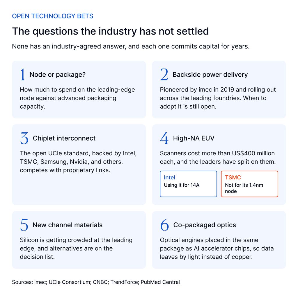
That script has multiplied, with what the ITRS treated as one line of development splintering into a set of parallel bets that do not share a schedule or a destination. A semiconductor CEO now has to weigh how much to spend on the leading-edge node against how much to put into advanced packaging capacity. Backside power delivery, pioneered by imec in 2019, is rolling out across the leading foundries, but when a company should adopt it remains an open question. Chiplet interconnect standards are splintering at the same time, with the open UCIe standard, which stands for Universal Chiplet Interconnect Express and is backed by Intel, TSMC, Samsung, Nvidia, and others, competing against proprietary alternatives. High-NA EUV scanners from ASML, which use high-numerical-aperture optics for the extreme ultraviolet wavelengths that have become the limiting tool for leading-edge chips, cost more than four hundred million dollars each, and the timing of the purchase decision matters as much as the decision itself. Intel and TSMC have already split on it. Intel is using High-NA to develop its 14A process, while TSMC has decided against it for its 1.4nm node. Silicon itself is getting crowded at the leading edge, with new channel materials and co-packaged optics for AI accelerators already on the decision list. None of these are questions with industry-agreed answers, some of the bets will turn out to have been right and others will not, and the skill required to live inside that uncertainty is different from the one the job asked for a decade ago.
The change in skill requirements has pushed boards to look beyond the traditional internal bench. Chief executive transitions across the industry’s integrated device manufacturers, pure-play foundries, and fabless designers have come faster over the last five years, and many have reached into adjacent parts of the semiconductor value chain, with leaders being pulled from electronic design automation (EDA) software firms, chip design intellectual property (IP) companies, and in a handful of cases from industries with no prior semiconductor exposure at all. The new profile still requires technical expertise, which is the price of entry, but it adds something harder to describe and harder to hire for. Boards are looking for capital-allocation judgment in an environment where the industry cannot reach consensus on the right answer, for credibility that holds across customers, regulators, and governments on three continents simultaneously, and for the stamina to lead a company through decisions whose correctness will not be visible for five or seven years after they are made.
What the Post-Moore Semiconductor C-Suite Now Looks Like Across Every Business Model
The leadership rebuild Moore’s Law has made necessary comes in eight versions, because the work the senior team does varies by the business model the company runs. An integrated device manufacturer (IDM), a pure-play foundry, a fabless designer, an outsourced semiconductor assembly and test (OSAT) company, an electronic design automation software firm, a chip intellectual property licensor, a semiconductor capital equipment maker, and a specialty materials and chemicals supplier each face a different version of the same physics, geopolitics, and capital intensity, and each is rebuilding the chief executive, chief technology officer, chief operating officer, chief financial officer, and chief human resources officer roles around its own pressures.
The same coordination problems run through all eight. The trilateral semiconductor export controls coordinated by the US, the Netherlands, and Japan reach into every business model. The regime continues to move, with the US Commerce Department clarifying at the end of May 2026 that its licensing requirements for advanced AI chips apply to any business headquartered in China or owned by a Chinese parent, wherever its subsidiaries operate. In September, Washington and Beijing extended their trade truce to January 10, 2027, with US officials keeping export controls off the negotiating table. A suspended US rule that would extend controls to companies at least 50% owned by listed entities is expected to stay paused until the same date. The cross-border fab integration challenges documented at projects in Arizona, Dresden, and Japan affect the equipment, materials, EDA, and IP suppliers as well as the foundries themselves, while the major industrial-policy programs across the US, Europe, Japan, and South Korea touch the capital decisions at IDMs, foundries, OSATs, and equipment makers. No single executive can sit credibly in every room the conditions now require, which is why the rest of this paper walks through what each role looks like inside each business model.
The Semiconductor CEO in a Post-Moore Industry
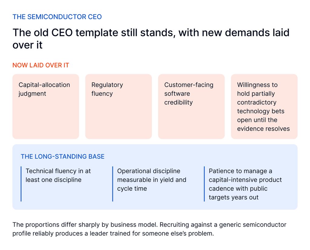
For most of the industry’s recent history, the traits that produced a successful semiconductor chief executive were well understood: technical fluency in at least one discipline, operational discipline measurable in yield and cycle time, and the patience to manage a capital-intensive product cadence with public targets years out. That template still stands, with new demands laid over it. Capital allocation judgment, regulatory fluency, customer-facing software credibility, and the willingness to hold partially contradictory technology bets open until the evidence resolves are now part of the role at every company in the industry, but the proportions in which they appear differ sharply by business model. Boards looking at CEO succession need to start from what the company’s business model demands, because recruiting against a generic semiconductor profile reliably produces a leader trained for someone else’s problem.
IDM CEOs
The integrated device manufacturer chief executive is running design, fabrication, and an external foundry business at the same time, against three subsidy regimes whose disbursement schedules and political conditions do not align. Intel’s appointment of Lip-Bu Tan in March 2025 gave the model its clearest test case, with an EDA-trained leader rebuilding both the product line and the foundry business at once. The rebuild has since moved below the top job, with Intel recruiting Seok-Hee Lee, the semiconductor veteran who previously ran SK hynix as its chief executive, in June 2026 as executive vice president of Intel Foundry. He leads advanced packaging, system integration, and back-end technology development and manufacturing, reporting directly to Tan.
What the role demands:
- Capital-allocation instinct sharp enough to commit billions to bets the industry itself cannot agree on.
- Sales conviction in front of foundry customers who are often direct product-line competitors.
- Subsidy fluency across the major industrial-policy programs, with the political instinct to read which conditions are negotiable.
Trust is the working content of the pure-play foundry chief executive’s job, and trust gets harder to hold when customers compete head-to-head in their own end markets. TSMC’s 2025 capital budget guidance of US$38 to US$42 billion gives a sense of the scale at which those decisions have to be defended, and the figure keeps climbing. In July 2026 the company raised its 2026 budget to between US$60 billion and US$64 billion, up from the US$52 billion to US$56 billion it had guided earlier in the year.
Foundry CEOs
Skill profile:
- The ability to keep equal trust with customers who are direct rivals.
- Equal credibility across Washington, Brussels, Tokyo, Seoul, and Taipei, in conversations whose participants increasingly know each other.
- A persuasive answer to how a Hsinchu-grown operating culture takes root in Phoenix, Dresden, or Kumamoto.
Fabless CEOs
A fabless chip is a software stack, a developer ecosystem, and a system architecture that happens to ship in silicon. The largest customers, the hyperscalers, increasingly maintain captive design teams of their own, which reframes the supplier relationship from component sale to system partnership.
What the role calls for:
- Working command of three conversations at once, transistor architecture, compiler and runtime software, and multi-year ecosystem commitment.
- A stance on selling into hyperscaler customers who behave like system partners and who increasingly build silicon in-house.
- The patience to fund developer-ecosystem investments whose returns surface three to five years out.
OSAT CEOs
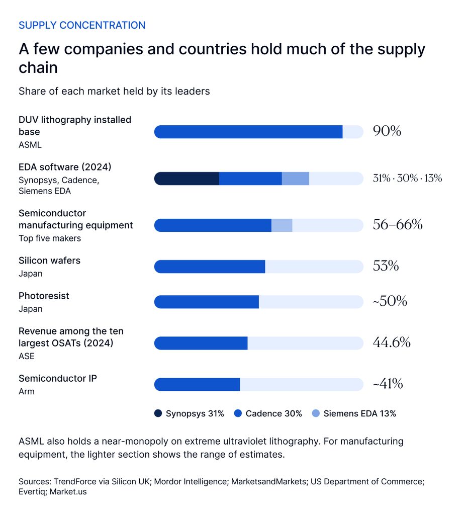
Outsourced semiconductor assembly and test was, for most of the industry’s history, a back-end service priced on volume. The leading OSATs now sit inside the technology bets that determine how AI accelerators perform commercially, with ASE holding 44.6% of revenue among the ten largest OSATs in 2024. Yole projected in 2025 that advanced packaging revenue would reach US$79.4 billion by 2030. Its 2026 update has since raised the outlook to more than US$120 billion by 2031, from US$55 billion in 2025.
What the role now requires:
- A clear technical position on which advanced packaging platforms to commit to, when the underlying physics is still settling.
- The capital nerve to underwrite multi-billion-dollar facilities against AI-accelerator demand whose volatility has been the defining feature of the last three years.
- Direct relationships with hyperscaler end customers, in parallel with the older foundry-intermediary relationships.
EDA CEOs
Three companies sell into nearly every chip project on the planet, and TrendForce’s 2024 figures put Synopsys at roughly 31% of the global market, Cadence at 30%, and Siemens EDA at 13%. AI-assisted design has changed the customer conversation over the last two years, with productivity gains consequential enough that customers now evaluate the EDA pipeline with the care they once reserved for the next process node.
Skill profile:
- Customer-relationship credibility across nearly every IDM, foundry, and fabless designer simultaneously.
- Pricing-model judgment when the underlying value of the tool is itself moving.
- Technical reach that bridges classical EDA algorithms and modern ML systems engineering, a combination almost no internal candidate pool has produced.
Chip IP CEOs
Arm, with roughly 41% of the semiconductor IP market, has been the dominant chip IP licensor for two decades. In March 2026 it began producing its own silicon for the first time in its history, with a data center CPU co-developed with Meta, which brings Arm closer to competing with some of the companies that license its designs. Its licensing business is also being tested by the rise of RISC-V and by hyperscaler design teams whose internal capabilities now let them choose between licensing and building.
What the job requires:
- A coherent answer to RISC-V, including which parts of the open-source threat to take seriously.
- Royalty pattern recognition across mobile, automotive, and AI inference end markets, none of which moves on the same cycle.
- Ownership of the broader ecosystem (software toolchains, security primitives, verification IP) that now matters to licensees as much as the core itself.
Equipment CEOs
A semiconductor equipment company’s standing rises and falls with the trade-policy temperature. ASML’s near-monopoly on extreme ultraviolet lithography, alongside 90% of the installed base of deep-ultraviolet tools, is the most visible position, and the top five equipment makers together hold roughly 56-66% of the manufacturing equipment market.
Skill profile:
- Equanimity with a customer base of fewer than twenty leading-edge fab operators, where one customer’s deferral can move the quarter.
- Working command of the trilateral US, Dutch, and Japanese export-control regime, plus the bilateral diplomacy that surrounds it.
- A profile boards have not historically priced for, closer to defense industrial leadership than to traditional B2B equipment sales.
Materials CEOs
Specialty materials and chemicals are the part of the semiconductor industry most exposed to single-source supply concentrations. According to figures cited by the US Department of Commerce, Japan holds about 53% of the global silicon wafer market and about 50% of the photoresist market, with supply concentrated in a small group of firms such as Shin-Etsu Chemical, SUMCO, JSR, and Tokyo Ohka Kogyo. Those concentrations turn the chief executive of a leading materials supplier into a participant in trade policy by virtue of what their company sells. China’s ban on helium exports in July 2026 showed how fast a single chipmaking input can turn into a trade-policy question.
What the role demands:
- Manufacturing discipline at part-per-billion purity, where a single contamination event can stop a customer’s line for weeks.
- Working understanding of how METI in Tokyo, Commerce in Washington, DG TRADE in Brussels, and MOTIE in Seoul each treat specialty materials as a national priority.
- The composure to give a credible public position when the company’s products are added to or removed from a control list.
The Semiconductor CTO Between Transistor Physics and System Architecture
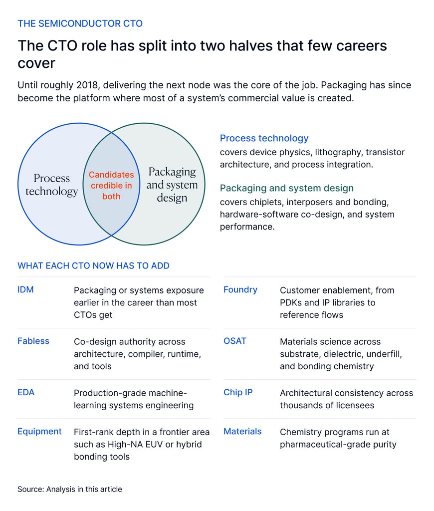
Until roughly 2018, a chief technology officer with a background in device physics, lithography, or transistor architecture could credibly oversee an R&D organization whose primary question was how to deliver the next process node on schedule. Two changes have since pulled the role apart. Process technology has fragmented into a set of parallel bets that do not share a schedule, and packaging has stopped being a back-end activity and become the platform on which most of the system’s commercial value gets created. The candidate pool that sits credibly across both halves is thinner than most org charts suggest.
IDM CTOs
The IDM chief technology officer is the only CTO in the industry running process technology, chip design, and packaging programs simultaneously, and the assumption that the three areas would progress on similar timelines has come apart. A process-technology career arc, the role’s historical feeder, does not cover what the job has become. Intel named Pushkar Ranade chief technology officer in July 2026, as part of a wider reshuffle of its senior team.
Profile of the role:
- Process technology depth sufficient to lead a multi-year R&D program from the front.
- Co-development experience with hyperscaler customers, including absorbing late-cycle architectural changes without losing the schedule.
- A career arc that combines device physics with packaging or systems exposure earlier than most CTO careers do.
Foundry CTOs
Process technology was the foundry chief technology officer’s domain for decades. Customer enablement (PDKs, IP libraries, reference flows, multi-project wafers, design service partnerships) has since taken equivalent priority on the calendar.
What the role asks for:
- Process depth that translates into the language a customer’s design team uses.
- A clear position on chiplet platforms (CoWoS, SAINT, the alternatives) and which to invest in next.
- Standing across customers whose scales differ by two orders of magnitude.
Fabless CTOs
A fabless chip is only as good as the software stack that runs on it. The cost of getting hardware-software co-design wrong on AI accelerators specifically is now severe, where the difference between a good and a bad implementation of a transformer kernel can move the effective performance of the silicon by an order of magnitude.
Skill profile:
- Co-design authority across the chip architecture, the compiler, the runtime, and the developer tooling, all four held in mind during the same product decision.
- Architectural standing against customers who maintain their own software teams capable of judging the work.
- Enough depth in transistor architecture and advanced packaging to make hardware-versus-system performance trade-offs.
OSAT CTOs
Hybrid bonding, panel-level packaging, fan-out wafer-level packaging, and chiplet integration each ask different things of substrate, dielectric, and underfill chemistry, and materials science is now at the center of the OSAT chief technology officer’s remit. Capital cycles commit those bets years before customer demand has resolved, which puts the role closer to a chemical-materials CTO than to a traditional OSAT operations technologist.
What the role demands:
- Materials science depth, the discipline now at the center of the role.
- Process development chops across substrate, dielectric, underfill, and bonding chemistries, running in parallel rather than sequentially.
EDA CTOs
Generative-AI offerings from the leading EDA vendors have moved from research projects into customer-facing products in roughly thirty months, and the chief technology officer is responsible for managing that transition without breaking the trust of customers whose chip projects span five-year horizons. By late 2026 all of the big EDA vendors were selling agentic AI tools for chip design. OpenAI and Synopsys went further in September, announcing GPT-Synopsys, a specialized model built to work with Synopsys design tools. The internal candidate pool for the role has thinned because the cross-disciplinary demands have outpaced what most EDA careers have produced.
Skill profile:
- Production-grade ML systems engineering, distinct from research-grade ML.
- Algorithmic depth across the classical EDA stack, synthesis, place-and-route, timing closure, formal verification.
- A cross-disciplinary career path the EDA industry has barely begun to produce internally.
Chip IP CTOs
Architectural consistency across thousands of licensees is the foundational discipline of the role, and the next generation of cores has to move forward without breaking it. Open-source pressure from RISC-V has changed the customer calculus, with licensees now able to choose between buying and building in a way they could not a decade ago.
What the role calls for:
- Release discipline that lets each new core generation ship without breaking software written for the last one.
- Technical judgment on how the company’s own cores should compete with, or sit alongside, RISC-V designs inside licensees’ chips.
Equipment CTOs
High-NA EUV, atomic-layer etching, hybrid bonding tools, and metrology systems for sub-2nm nodes each require R&D programs measured in billions of dollars and decades of effort, on behalf of customers who themselves do not know exactly when they will need the next tool.
Skill profile:
- Willingness to commit to high-risk physical R&D bets when development cycles run for decades.
- First-rank domain depth in at least one frontier area (high-NA EUV, atomic-layer etching, hybrid bonding tools, sub-2nm metrology).
Materials CTOs
Chemistry programs at the materials CTO level operate at purity levels closer to pharmaceutical manufacturing than to traditional industrial chemistry, and the rest of the industry’s progress depends on whether the major chemistries (EUV photoresists, ALD precursors, CMP slurries, bonding chemistries) clear that bar.
What the role demands:
- A chemistry program run at pharmaceutical-grade purity, with the regulatory and quality systems that come with that standard.
- Defensible IP across the US, EU, Japan, Korea, and Taiwan.
- Trade-policy assessment built into platform-investment decisions from the start, not appended afterwards.
The Semiconductor COO and the New Operational Complexity of Multi-Node Manufacturing
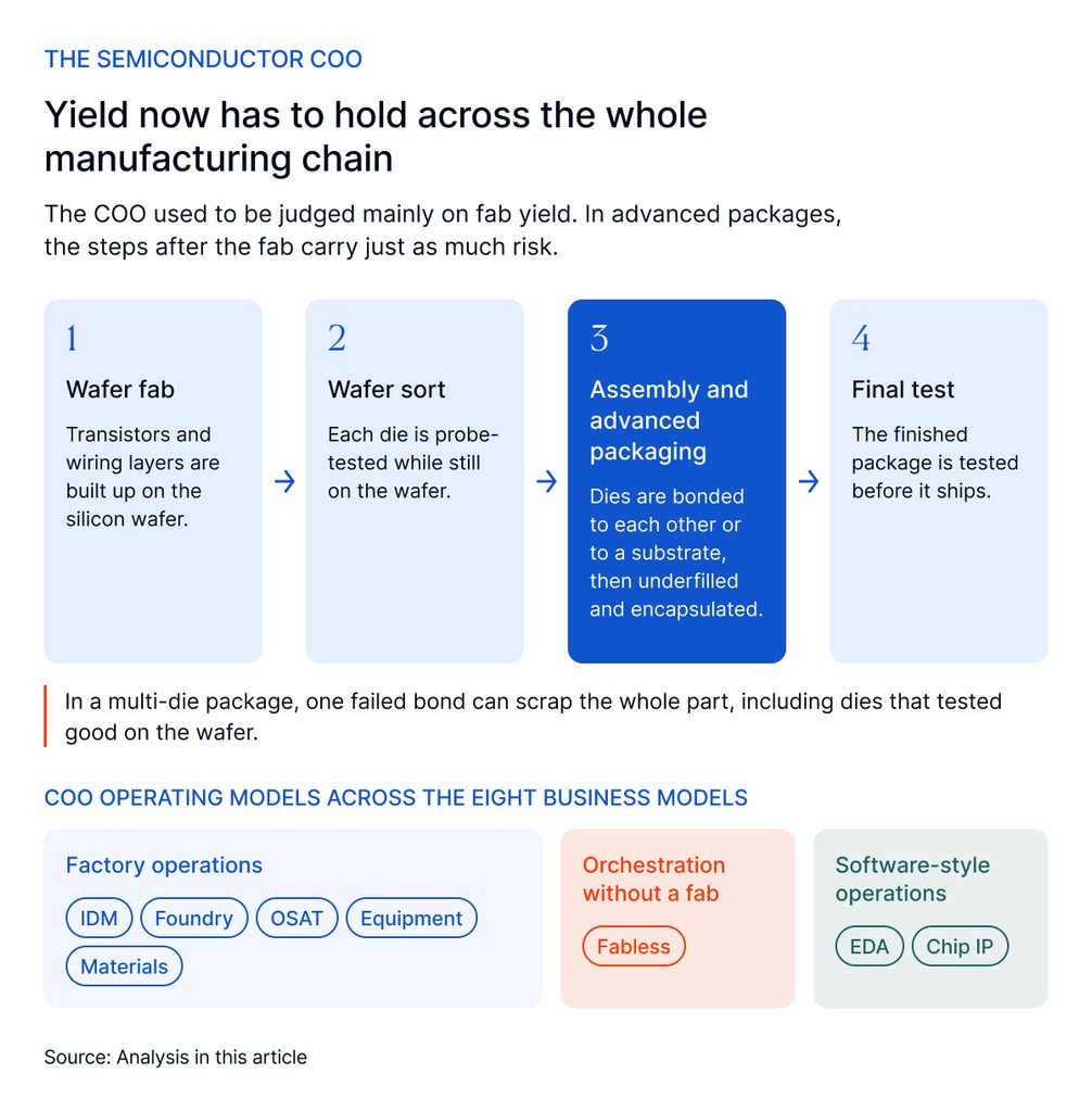
Yield used to be the chief operating officer’s domain, defined by cycle time, defect density, and equipment utilization on a product mix that did not change often. Operational discipline of that kind is still necessary at every company in the industry, and at none of them is it sufficient. Yield has become a package-level question in many parts of the industry, advanced packaging has put materials science back in the operations function’s path, and the geographic footprint of manufacturing has multiplied.
IDM COOs
Wafer fab, sort, assembly, test, and increasingly advanced packaging all sit inside the IDM chief operating officer’s span, with a footprint spread across the US, Europe, Asia, and emerging Middle Eastern sites. Yield is now a system-level question that often includes foundry-supplied dies for products the IDM chooses not to make internally.
What the role demands:
- Comfort running a hybrid manufacturing model, some products end-to-end internal, others partially outsourced.
- System-level yield ownership across fab, sort, assembly, test, and packaging as a single chain.
- A clear position on the internal politics of capacity sharing between the IDM’s product business and external foundry customers.
Foundry COOs
Dozens of customers compete for slots on the same leading-edge nodes, capital decisions take three to five years to translate into wafers, and customer prepayments lock in capacity long before the demand it serves has resolved. The chief operating officer balances those commitments against actual demand on a continuous basis.
Skill profile:
- Temperament to allocate scarce capacity among dozens of competing customers without breaking trust with any of them.
- Customer-prepayment mechanics, and the commercial logic of locking in capacity well before demand has resolved.
- The ability to translate an operating culture cleanly across geographies whose labor markets, supplier ecosystems, and regulatory frameworks differ in material ways.
Fabless COOs
Fabless operations does not touch a wafer, which has nothing to do with how hard the job is. Supply-chain orchestration across foundries and OSATs, allocation fights against customer priorities that compete with the company’s own, and inventory management against post-2020 demand volatility now define the role.
What the job demands:
- Personal relationships with foundries and OSATs whose decisions determine the fabless company’s product trajectory.
- Negotiating instinct against competing customer priorities, particularly when the largest competitor for capacity is the foundry’s anchor customer.
- Product transition planning across nodes whose timing customers may not be ready for.
OSAT COOs
Final-package yield depends on a chain of bonding, underfill, encapsulation, and testing steps, any of which can drop the result to zero even when every die going in is good. Hybrid bonding, fan-out wafer-level packaging, and chiplet integration have grown that chain sharply over the last decade.
Skill profile:
- Yield ownership at the package level across hybrid bonding, fan-out wafer-level, and chiplet integration flows.
- Operational instinct for a multi-step assembly process where any one step can drop final yield to zero.
- Continued attention to cycle time, capacity utilization, and defect density at traditional metrics, alongside the system-level yield problem.
EDA COOs
EDA operations is closer to SaaS operations than to manufacturing operations, and the talent flowing into the function reflects that. Customer support across hundreds of large licensees, license server reliability, cloud tool deployment, professional services delivery, and the continuous integration pipelines that hold the toolchain together fill the chief operating officer’s working week.
What the role demands:
- SaaS-style operational instinct, sized to enterprise-software volumes.
- Customer support coverage across hundreds of licensees, each of which is also a key relationship the EDA CEO is personally managing.
- Technical literacy to keep cloud-delivered tooling and on-premise license models running cleanly in parallel.
Chip IP COOs
Chip IP operations exists to do three things: ship verified IP to licensees, account for royalties against an installed base in the billions of devices, and run the verification programs that protect the company’s reputation across every node and process the IP gets ported to. Quality at the IP level has consequences that propagate through every customer’s product.
Skill profile:
- Royalty accounting on an installed base measured in billions of devices.
- Ownership of the verification and qualification programs that have to clear cleanly across every node and process the IP gets ported to.
- Delivery cadence to keep up with customer product cycles that have shortened over the last five years.
Equipment COOs
Lead times for semiconductor equipment are measured in years, not quarters. An EUV scanner takes the better part of a year to assemble before the tool ships, drawing on a multi-tier global supplier ecosystem whose qualification standards are themselves the work of years.
What the job calls for:
- Comfort with manufacturing lead times measured in years, and the customer planning rhythms that come with them.
- Coordinative skill across a multi-tier global supplier ecosystem in which any one component can hold up an entire tool shipment.
- Field service expertise covering customer installations across the global fab base, where on-site teams often live inside the customer’s facility for months.
Materials COOs
Customers in this part of the industry will reject batches over trace contaminations that less demanding industries would never detect. New Korean, Taiwanese, and US production lines are coming online in parallel, each adding its own regulatory interface to the operations function.
Skill profile:
- Batch-to-batch consistency at part-per-billion purity, with the contamination-control programs to sustain it.
- A primary operational metric that is invisible most of the time, namely how often the company has caused a customer line stoppage
- Direct working relationships with regulators in multiple national jurisdictions, each treating specialty materials as a national priority.
The Semiconductor CFO Under Rock’s Law
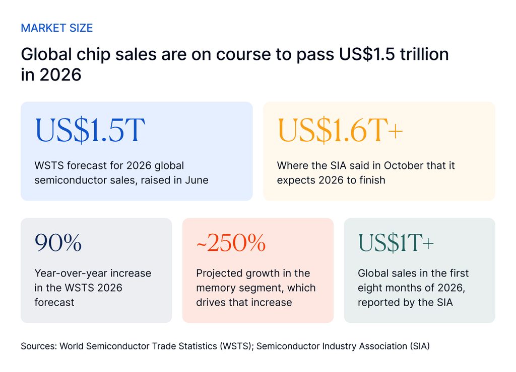
Capital intensity has always been the central feature of the chief financial officer role, and Rock’s Law has not been kind to the predictability that used to come with it. Capital intensity has risen, payback windows have lengthened, and subsidy schedules have introduced a political variable into long-term financial planning that the role did not use to carry. The demand side has become no easier to model, with the World Semiconductor Trade Statistics organization raising its 2026 forecast in June to US$1.51 trillion in global sales, a 90% year-over-year increase driven by a memory segment projected to grow by around 250%. Even that figure now looks conservative. The SIA reported in October that sales had passed US$1 trillion in the first eight months of the year and that it expects 2026 to finish above US$1.6 trillion. The CFO at each of the eight business models is now underwriting a multi-year capital story whose payoff is further out than most other capital projects in the global economy.
DM CFOs
The IDM chief financial officer commits capital to node development, packaging capacity, and external foundry capacity simultaneously, each stream with its own payback profile. The role is increasingly the seat from which the integrated model itself is judged to be working or not.
What the role demands:
- Underwriting instinct for multi-decade capital commitments against subsidy windows that may close.
- Working command of three different capital streams running in parallel (node, packaging, foundry capacity).
- Treasury, tax, and customer-finance reach across multiple jurisdictions whose authorities increasingly compare notes.
Foundry CFOs
A foundry runs one of the most capital-intensive financial models in the global economy, and the chief financial officer holds the levers (customer prepayments, government subsidies, and depreciation schedules) that determine whether the company stays profitable.
Skill profile:
- Customer-prepayment and capacity-pricing mechanics at the scale leading-edge foundry contracts now require.
- A defensible position on depreciation schedules across both book and tax authorities in multiple jurisdictions.
- Financial nerve to underwrite annual capex commitments now running into the tens of billions, against demand that may not fully materialize.
Fabless CFOs
A fabless company is asset-light in everything except R&D, and R&D commitments behave more like capital expenditure than like operating cost on the chief financial officer’s underwriting model. R&D can run to a quarter or more of revenue at the leading fabless designers, and the CFO has to defend that against quarterly profit pressure.
What the role calls for:
- Financial discipline to defend R&D investment levels at a quarter or more of revenue.
- Risk modeling for a customer base in which a single hyperscaler can move quarterly revenue and may also commission competing silicon.
- A defensible model for the AI investment cycle currently driving sector growth, including what happens if it softens.
OSAT CFOs
Moderate capex, stable customer relationships, and predictable utilization curves were the financial signature of the OSAT chief financial officer’s job for most of its history. Amkor’s Arizona advanced packaging campus, announced at US$7 billion in 2025 and expanded to about US$12 billion in September 2026, has joined parallel investments by other leading OSATs in moving the underwriting question into territory the role used to leave to foundries.
Skill profile:
- Capex underwriting at facility scales the role did not use to see.
- An AI-accelerator demand model good enough to inform pricing and capacity-commitment decisions on advanced packaging.
- Yield-curve modeling for packaging platforms that have little production history to model from.
EDA CFOs
A decade of subscription transition has changed the EDA chief financial officer’s job, and AI-augmented tooling has now added a usage-based pricing layer on top of the seat count. M&A has been a regular feature of the role, with Synopsys’ US$35 billion acquisition of Ansys, completed in July 2025, the largest in EDA history.
What the role calls for:
- Subscription accounting at enterprise-software scale, including multi-year backlog visibility.
- Two pricing models running in parallel, the older seat-count subscription and the newer usage-based AI-tooling layer.
- Integration experience for large M&A, since the next round of consolidation is unlikely to be smaller.
Chip IP CFOs
Royalty income tied to the unit shipments of customers’ end products defines the chip IP chief financial officer’s revenue model, and a small number of large customers drive disproportionate variance.
Skill profile:
- Reading royalty cycles in three end markets at once, mobile, automotive, and AI inference, none of which moves on the same cadence.
- RISC-V adoption modeled as a category-level risk, regardless of its near-term effect on royalty revenue.
- A career profile closer to a payments-network CFO than to a traditional software finance leader.
Equipment CFOs
Fewer than twenty leading-edge fab operators make up the customer base of a semiconductor equipment chief financial officer, and the loss of any single customer’s order cycle can move quarterly revenue by hundreds of millions of dollars. Long sales cycles, pre-order deposits, and revenue recognized at tool installation combine into a forecasting model whose accuracy depends on a handful of customer programs going to plan.
What the job demands:
- Steady judgment in the face of a customer-risk profile no other industrial finance function carries.
- Long sales cycles, pre-order deposits, and the cash-management implications of receiving large payments years before recognition.
- Forecasting that absorbs export-control variation, where the proportion of revenue requiring government licensing changes from quarter to quarter.
Materials CFOs
Pricing power in a specialty materials business comes from customer qualification depth and supply concentration rather than from volume scale. Capital investments such as Tokyo Ohka Kogyo’s South Korean photoresist plant scheduled for 2030 have to be underwritten against trade-policy outcomes the company cannot directly influence.
Skill profile:
- Financial command of a manufacturing model whose pricing power comes from qualification depth and supply concentration rather than raw volume.
- Underwriting instinct for capital investments whose outcomes depend in part on trade-policy decisions the company cannot influence.
- Scenario analysis that builds export-control regimes into the financial planning model as a routine variable.
The Semiconductor CHRO and the Succession Problem Moore’s Law Hid
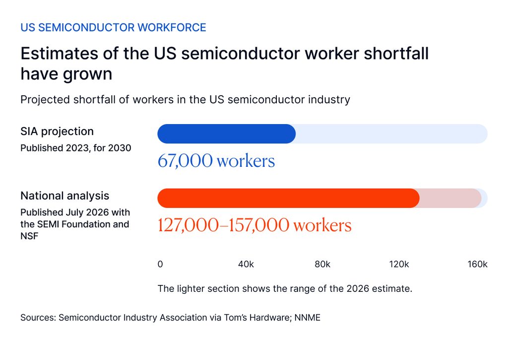
Few executive roles in the industry have changed more in five years than the chief human resources officer’s. Moore’s Law did most of the leadership-development work for the function, with careers progressing against an industry-wide schedule that selected its own candidates and benches that filled themselves. When the cadence broke, the hidden weakness of the system became visible, and the broader US workforce shortage sits underneath each of the eight business-model rebuilds. That shortage has grown on paper as well as in practice. In 2023 the SIA projected a shortfall of 67,000 workers in the US semiconductor industry by 2030, and a July 2026 national analysis published with the SEMI Foundation and the National Science Foundation has since put the figure at 127,000 to 157,000 workers.
IDM CHROs
The IDM chief human resources officer is rebuilding two workforces at once, one inside the older internal-product culture and one staffing the foundry business whose customer-service demands the company has to learn from scratch. The candidate pool that has done that kind of integration sits largely outside the semiconductor industry.
What the role demands:
- Experience running two workforce cultures side by side without letting either one absorb the other.
- Recruiting reach into foundry competitors at the moment those competitors are themselves expanding.
- Cross-industry recruitment instincts, since the internal candidate pool for customer-foundry leadership is thin and unlikely to thicken on its own.
Foundry CHROs
Foundry expansions to Arizona, Dresden, and Kumamoto each require the translation of an operating model built around a particular Taiwanese working culture into very different local labor markets, and the chief human resources officer is the executive responsible for that translation. Cross-border talent partnerships such as the Taiwan-Germany semiconductor talent collaboration have begun to address the engineering pipeline.
Skill profile:
- Hands-on experience integrating an operating culture into local labor markets whose expectations about hours, hierarchy, and engineering standards differ in material ways.
- A clear theory of which parts of the home operating model must travel unchanged and which can adapt to local norms.
- Sustained attention to the supervisor and middle-manager cultural integration question, where most cross-border operational friction lives.
Fabless CHROs
Fabless talent acquisition is now in direct competition with the hyperscalers who used to be customers, for the same scarce pool of AI architects, compiler engineers, and senior individual contributors at compensation levels approaching Big Tech.
What the role demands:
- AI talent acquisition and retention against hyperscaler compensation.
- A defensible position on how the compensation budget gets divided between top-end individual contributors and the broader bench.
- Recruiting credibility against companies that can pay more and increasingly want the same people.
OSAT CHROs
OSAT human resources used to mean a workforce concentrated in lower-wage assembly operations and a smaller engineering bench focused on packaging process development. Advanced packaging has changed the talent profile, with hybrid bonding and chiplet integration each demanding specialty engineers whose skills overlap with front-end fab and materials science.
Skill profile:
- Specialty packaging engineer recruiting against IDM and foundry competitors who can pay more.
- A talent strategy spanning assembly process, front-end fab process, and materials science.
- A plan to steer the workforce mix toward something more closely resembling a foundry engineering bench.
EDA CHROs
EDA hiring used to concentrate on classical algorithm engineers, formal-verification specialists, and customer-facing applications engineers. AI-augmented tooling has added a new and very expensive talent category, with the same machine-learning researchers the frontier labs are competing for now appearing on EDA shortlists.
What the role calls for:
- Recruiting reach into the same machine-learning researcher pool the frontier labs are hiring from.
- Retention skill on the classical EDA bench during a transformation that has unsettled established career paths.
- A dual-track talent strategy, classical EDA engineering and ML systems engineering, in parallel for as long as the toolchain transition takes.
Chip IP CHROs
Senior architects in a chip IP company are functionally irreplaceable on short notice. Hyperscaler captive design teams can pay individual architects more than a public IP company typically offers, which makes retention a recruiting problem run in reverse.
Skill profile:
- A retention plan for senior architects that holds against hyperscaler captive design team offers.
- Long-horizon planning for a profession in which the most senior practitioners cannot be replaced on short notice.
- The patience to identify and develop architects in their thirties for roles they will not hold until their fifties.
Equipment CHROs
Senior engineers in semiconductor equipment, in disciplines such as precision optics, plasma physics, ultra-clean materials handling, and ion-beam metrology, take a decade or more to develop. Some specializations have only dozens of senior practitioners worldwide.
What the role demands:
- Pipeline planning measured in decades for engineers in narrow disciplines.
- Retention focus on senior individual contributors in fields with sometimes only dozens of senior practitioners worldwide.
- Contingency planning for the single-loss risk in narrow technical specializations, since one departure can move R&D timelines by quarters.
Materials CHROs
Chemists, materials scientists, and process engineers work inside customer qualifications that take years to complete and are not transferable across customers. New facilities in Korea, Taiwan, and the US each have to be staffed largely from scratch in the local market while remaining qualified to the same standards as the home country.
Skill profile:
- Workforce planning that protects customer qualifications when a senior chemist or process engineer leaves.
- Greenfield staffing experience across Korea, Taiwan, and the US in parallel.
Which Semiconductor Business Models Face the Hardest Leadership Rebuild?
Two patterns emerge from running through the eight business models in turn. The first is that the rebuild is hardest at the IDM, the foundry, and the OSAT. Each of those three businesses now combines capital intensity, geographic dispersion, and customer-concentration pressures of a kind no single career has typically produced a leader fluent in. The fabless and chip IP businesses face serious but more bounded rebuilds, mostly concentrated in the chief executive and chief technology officer roles where the customer relationship has changed character. The EDA, equipment, and materials businesses start from a position of greater stability at the top, partly because their customer concentration was already a defining feature of the role rather than a recent shock to it. Their pressure sits mostly lower down, in CTO and CHRO seats whose candidate pools are among the thinnest in the industry.
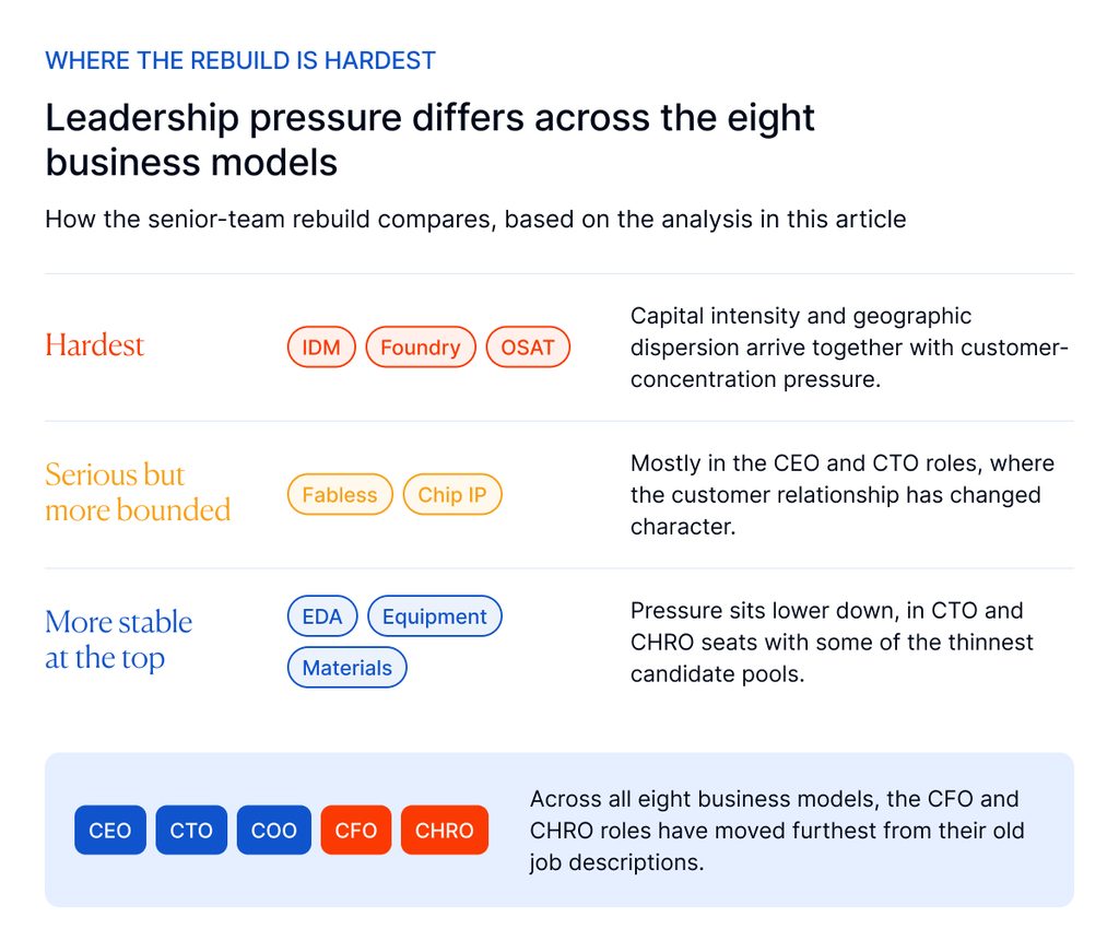
The second pattern concerns the roles. Across the eight business models, the chief financial officer and chief human resources officer roles have moved furthest from their old job descriptions, because those descriptions assumed a degree of internal predictability that has since gone. The CFO is now underwriting capital programs whose risk profile sits well outside what most semiconductor finance careers were built around, and the CHRO is rebuilding leadership pipelines whose original feeder process Moore’s Law itself was supplying. Boards looking at the next succession cycle tend to focus on the chief executive and the chief technology officer. They should give the CFO and CHRO appointments the same attention, because those two seats show earliest whether the company is positioned for what comes next.
What Boards Should Do Before Their Next Semiconductor Executive Transition
None of this is comfortable, particularly for an industry whose sense of its own leadership was built by engineers who came of age inside a system that rewarded them for doing one thing extraordinarily well. That system is being dismantled by physics, by industrial policy, and by demography, and it is being dismantled at a different pace inside each of the eight business models the industry now contains. The question for boards is whether the leadership rebuild will be finished in time for the succession cycles already on the horizon. Those cycles are closer than most succession plans allow for, and the external candidates who can meet the new profile are being recruited by every adjacent sector with similar pressures at the same time.
Seven things are worth putting on the board’s agenda before the next transition.
- Rewrite the role specifications against the company’s business model first. Hiring criteria for the CEO, CTO, COO, CFO, and CHRO should be rebuilt against the post-Moore profile that fits the specific business model, before any candidate shortlist is drawn up. A specification written for an IDM CEO will not produce a foundry candidate, a fabless specification will not produce an OSAT one, and a job description copied across business models will reliably produce a leader prepared for the wrong set of pressures.
- Start bench-building two and three levels below the executive committee now. Waiting until a succession event to identify a successor leaves the bench too thin to draw from under time pressure. The companies most likely to come through the next decade in good condition will be the ones that began grooming two or three potential chief executives five years before they needed them, and that built formal rotational programs rather than relying on the accidental development that used to be sufficient when the cadence itself did most of the selecting.
- Build cross-regional rotation into the development path before general management, not after it. A high-potential manager trained in Hsinchu will not automatically read the political logic of a Brussels State aid package, a Dresden-trained engineer will not automatically grasp the hiring realities of Taylor, Texas, and an Arizona fab leader will not automatically anticipate the cultural norms governing a Kumamoto operation. Rotating future leaders across at least two geographies and three functional areas adds years to the development timeline for each executive, and boards should price that reality into their succession planning now rather than later.
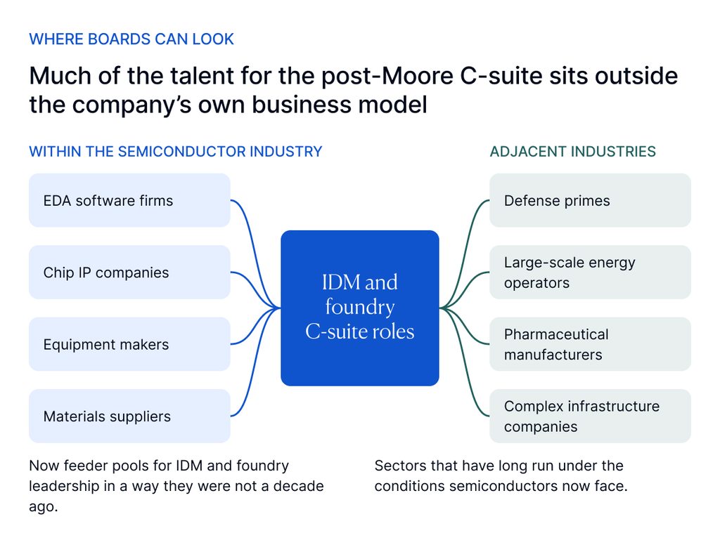
- Expand the candidate aperture beyond semiconductors and across business models. The adjacent industries that have been running under the conditions semiconductors now face (defense primes, large-scale energy operators, pharmaceutical manufacturers, and complex infrastructure companies) are where much of the external talent fit for the post-Moore C-suite sits. Within the industry itself, EDA, IP, equipment, and materials companies are now feeder pools for IDM and foundry C-suite roles in a way they were not a decade ago. Boards that limit shortlists to candidates with prior experience in their own business model will miss most of the pool.
- Pressure-test the succession plan against a compressed timeline. Health events, recruitment by a competitor, or a governance dispute can shrink a five-year succession timeline into a five-month one. A plan that looks adequate on paper often does not survive that compression, and the time to discover that is not at the point of the next transition.
- Audit the board’s own expertise against the profile being hired for. A board whose members all came up through the same era of the industry will struggle to assess a candidate whose background sits outside it, and adding a director with experience in defense, energy, or pharmaceutical capital allocation, or in a different semiconductor business model than the company’s own, is often the precondition for making an external hire later.
- Treat the CHRO appointment as the precondition for everything else. The CHRO role is where the leadership rebuild the whole paper has been describing either happens or does not. That makes it the role most in need of board attention during the next transition cycle, and the one where the instinct to treat HR as a support function rather than a succession-defining appointment will cost the company the most.
About the Authors
Jan-Bart Smits is a Managing Partner at Stanton Chase Amsterdam and leads the firm’s global Technology sector and its Semiconductors subsector. He has worked in executive search since 1990 and runs Stanton Chase’s Global Semiconductor Practice. Over that time, he has led numerous CxO and non-executive board assignments. He previously served as the firm’s Global Chair and has published semiconductor thought leadership through industry bodies such as SEMI. His work spans Technology and Professional Services, with functional expertise in Marketing and Sales and CFO and Financial Executives appointments. He holds an MSc in astrophysics from Leiden University.
Sundar Rajan Ramalingam is a Partner at Stanton Chase Baltimore and part of the firm’s North American semiconductor practice. He joined Stanton Chase after nearly three decades in manufacturing and global technology, where he moved from HR leadership into general management. His search work focuses on Technology Executives and Private Equity mandates in Technology and Industrial companies. He holds an MBA from XLRI Jamshedpur.
David Harap is a Managing Director at Stanton Chase Austin, with more than 25 years of experience in senior-level executive search. His industry focus is Technology, especially emerging technologies, along with Life Sciences and Healthcare. On the functional side, he concentrates on CEO Search and Succession and CFO and Financial Executives appointments. He lectures at the University of Texas at Austin and is a certified Hofstede Insights Ambassador. He holds a B.Sc. in industrial and labor relations from Cornell University.
How Can We Help?
At Stanton Chase, we're more than just an executive search and leadership consulting firm. We're your partner in leadership.
Our approach is different. We believe in customized and personal executive search, executive assessment, board services, succession planning, and leadership onboarding support.
We believe in your potential to achieve greatness and we'll do everything we can to help you get there.
View All Services